ECP5 QUAD Wrapper
This module wraps around the IP generated by Diamond for instantiating up to two ECP5 PCS Dual IP cores, also referred to as DCUs (Dual Channel Units). This module instantiates one or two ECP5 PCS Dual IP cores based on which channels are enabled through the rx_enable_g and tx_enable_g generics. Each dual contains two channels, and each channel contains separate data paths for transmission (TX) and reception (RX). The two channels of a given dual are not completely independent as they share a single PLL for the TX path, however the channels between two duals are independent.
By default, all channel enables are set to 1 and the module instantiates two ECP5 PCS Dual IP cores. The width of the high-speed serial input and output ports of the module (hdin/hdout) depends on the number of duals that contain at least one enabled channel. If only one dual is needed, they will be 2-bit wide, otherwise they will be 4-bit wide. These ports and some generics (such as the enables and the invert) contain information that relates to the four channels; when this happens, the channel each bit is referred to is determined positionally in the order “ch3 downto ch0”. Similarly, if a generic vector refers to both duals, it does so in the order “dcu1 downto dcu0”.
For each channel, this module provides a user-facing 8-bit datapath with 8b/10b K-character control, Built-In Self Test (BIST) hooks, diagnostic counters, and reset sequencing around the underlying transceiver primitive.
The wrapper has several build-time configurations presented as optional generic parameters to accommodate various use cases. These are discussed in the “Configuring the Quad Wrapper” section below.
This module does not support every possible configuration of the PCS IP core. If the requirements of the application are incompatible with the provided settings and interfaces, a direct instantiation of the pcs IP core in the Diamond tool Clarity Designer or even a direct instantiation of the DCUA primitive from the Lattice ECP5UM components library may be preferred. However, HotRIO connections are always supported by the Quad Wrapper, either directly or through the Dual Ring Wrapper.
Detailed portlist
Generics
Name |
Description |
Type |
Default |
|---|---|---|---|
dcu_frequency_g | set tx byte clock frequencies for serdes/pcs duals in the order d1 downto d0. valid options: freq_40, freq_125, freq_250 |
|
|
dlink_rx_channels_g | rx channels to be directly linked to dual transmitters in the order d1 downto d0. set to numbers in [0, 3] to enable the direct links |
|
|
rx_enable_g | enable rx channels. a zero removes the rx channel instance from the module |
|
|
tx_enable_g | enable tx channels. a zero removes the tx channel instance from the module |
|
|
rx_invert_g | invert rx serial data inputs |
|
|
tx_invert_g | invert tx serial data outputs |
|
|
dcu_lol_size_g | set the log2 of the no. of tx_refclk cycles over which the differences below are accumulated |
|
|
dcu_unlock_diff_g | set the min difference in no. of tx_refclk and tx_pclk rising edges to consider the txpll unlocked |
|
|
dcu_lock_diff_g | set the max difference in no. of tx_refclk and tx_pclk rising edges to consider lock recovered |
|
|
rx_serdes_rst_bits_g | log2 of the no. of clock cycles to wait to change state after lock of the cdr |
|
|
rx_pcs_rst_bits_g | log2 of the no. of clock cycles to wait to change state after release of the serdes rx reset |
|
|
rx_pcs_lock_bits_g | log2 of the no. of consecutive clock cycles with locked cdr before considering the rx channel ready |
|
|
rx_pcs_lol_bits_g | log2 of the no. of consecutive clock cycles with unlocked cdr before restarting the rx reset sequence |
|
|
rx_err_cnt_bits_g | log2 of the no. of rx errors every 2^17 cycles at which a rx pcs reset is issued |
|
|
tx_serdes_rst_bits_g | log2 of the no. of clock cycles to wait to change state after lock of the txpll |
|
|
tx_pcs_rst_bits_g | log2 of the no. of clock cycles to wait to change state after release of the serdes tx reset |
|
|
tx_pcs_lock_bits_g | log2 of the no. of consecutive clock cyles with locked txpll before considering the tx dual ready. must be higher than `dcu_lol_size_g` |
|
|
tx_pcs_lol_bits_g | log2 of the no. of consecutive clock cycles with unlocked txpll before restarting the tx reset sequence. must be higher than `dcu_lol_size_g` |
|
|
bist_k_counter_bits_g | log2 of the no. of full bist ramps between two replacements of the d0.0 with k28.5 |
|
|
Input signals
IN ports
Name |
Description |
Type |
|---|---|---|
hdinp | serial stream input for the four channels (true ports) |
|
hdinn | serial stream input for the four channels (complement ports) |
|
dcu0_clk_i | system clock for dual 0. frequency must match `dcu_frequency_g(0)` |
|
dcu0_rstn_i | active low synchronous reset signal for dual 0 |
|
dcu0_tx_sync_i | resets all the tx serializers of dual 0, used to align ch0 and ch1 transmissions |
|
dcu1_clk_i | system clock for dual 1. frequency must match `dcu_frequency_g(1)` |
|
dcu1_rstn_i | active low synchronous reset signal for dual 1 |
|
dcu1_tx_sync_i | resets all the tx serializers of dual 1, used to align ch2 and ch3 transmissions |
|
ch0_rx_pwrup_i | ch0 rx power-up |
|
ch0_tx_pwrup_i | ch0 tx power-up |
|
ch0_tx_idle_i | disable serial output of ch0 (pcie electrical idle state) |
|
ch0_tx_data_i | ch0 tx data |
|
ch0_tx_kchar_i | ch0 tx k-character flag |
|
ch0_tx_disp_correct_i | fix the disparity for ethernet communications. only use while sending the data character of idle2 |
|
ch0_tx_force_disp_i | force the disparity in the ch0_tx_disp_sel input |
|
ch0_tx_disp_sel_i | select the disparity to be used in the tx data (if forced) |
|
ch0_bist_en_i | enable bist for ch0 |
|
ch1_rx_pwrup_i | ch1 rx power-up |
|
ch1_tx_pwrup_i | ch1 tx power-up |
|
ch1_tx_idle_i | disable serial output of ch1 (pcie electrical idle state) |
|
ch1_tx_data_i | ch1 tx data |
|
ch1_tx_kchar_i | ch1 tx k-character flag |
|
ch1_tx_disp_correct_i | fix the disparity for ethernet communications. only use while sending the data character of idle2 |
|
ch1_tx_force_disp_i | force the disparity in the ch1_tx_disp_sel input |
|
ch1_tx_disp_sel_i | select the disparity to be used in the tx data (if forced) |
|
ch1_bist_en_i | enable bist for ch1 |
|
ch2_rx_pwrup_i | ch2 rx power-up |
|
ch2_tx_pwrup_i | ch2 tx power-up |
|
ch2_tx_idle_i | disable serial output of ch2 (pcie electrical idle state) |
|
ch2_tx_data_i | ch2 tx data |
|
ch2_tx_kchar_i | ch2 tx k-character flag |
|
ch2_tx_disp_correct_i | fix the disparity for ethernet communications. only use while sending the data character of idle2 |
|
ch2_tx_force_disp_i | force the disparity in the ch2_tx_disp_sel input |
|
ch2_tx_disp_sel_i | select the disparity to be used in the tx data (if forced) |
|
ch2_bist_en_i | enable bist for ch2 |
|
ch3_rx_pwrup_i | ch3 rx power-up |
|
ch3_tx_pwrup_i | ch3 tx power-up |
|
ch3_tx_idle_i | disable serial output of ch3 (pcie electrical idle state) |
|
ch3_tx_data_i | ch3 tx data |
|
ch3_tx_kchar_i | ch3 tx k-character flag |
|
ch3_tx_disp_correct_i | fix the disparity for ethernet communications. only use while sending the data character of idle2 |
|
ch3_tx_force_disp_i | force the disparity in the ch3_tx_disp_sel input |
|
ch3_tx_disp_sel_i | select the disparity to be used in the tx data (if forced) |
|
ch3_bist_en_i | enable bist for ch3 |
|
Output signals
OUT ports
Name |
Description |
Type |
|---|---|---|
hdoutp | serial stream outputs for the four channels (true ports) |
|
hdoutn | serial stream outputs for the four channels (complement ports) |
|
dcu0_tx_ready_o | common tx ready signal for dual 0 |
|
dcu1_tx_ready_o | common tx ready signal for dual 1 |
|
ch0_rx_clk_o | ch0 recovered clock (if locked) |
|
ch0_rx_ready_o | ch0 rx ready signal |
|
diag_ch0_rx_err_cnt_o | number of running disparity and code violation errors received on ch0 since last pcs reset |
|
ch0_rx_data_o | ch0 rx data |
|
ch0_rx_kchar_o | ch0 rx k-character flag |
|
ch0_bist_active_o | signals that the bist initialization has been received |
|
ch0_bist_err_o | pulses high when an error is detected in the received bist |
|
ch1_rx_clk_o | ch1 recovered clock (if locked) |
|
ch1_rx_ready_o | ch1 rx ready signal |
|
diag_ch1_rx_err_cnt_o | number of running disparity and code violation errors received on ch1 since last pcs reset |
|
ch1_rx_data_o | ch1 rx data |
|
ch1_rx_kchar_o | ch1 rx k-character flag |
|
ch1_bist_active_o | signals that the bist initialization has been received |
|
ch1_bist_err_o | pulses high when an error is detected in the received bist |
|
ch2_rx_clk_o | ch2 recovered clock (if locked) |
|
ch2_rx_ready_o | ch2 rx ready signal |
|
diag_ch2_rx_err_cnt_o | number of running disparity and code violation errors received on ch2 since last pcs reset |
|
ch2_rx_data_o | ch2 rx data |
|
ch2_rx_kchar_o | ch2 rx k-character flag |
|
ch2_bist_active_o | signals that the bist initialization has been received |
|
ch2_bist_err_o | pulses high when an error is detected in the received bist |
|
ch3_rx_clk_o | ch3 recovered clock (if locked) |
|
ch3_rx_ready_o | ch3 rx ready signal |
|
diag_ch3_rx_err_cnt_o | number of running disparity and code violation errors received on ch3 since last pcs reset |
|
ch3_rx_data_o | ch3 rx data |
|
ch3_rx_kchar_o | ch3 rx k-character flag |
|
ch3_bist_active_o | signals that the bist initialization has been received |
|
ch3_bist_err_o | pulses high when an error is detected in the received bist |
|
Configuring the Quad Wrapper
Dual Ring mode
A partially preconfigured Quad Wrapper for the HotRIO Dual Ring network architecture is available by instantiating ecp5_dual_ring_wrapper instead of ecp5_quad_wrapper. A description of the portlist and usage of this auxiliary module is provided in the dedicated page:
Supported line rates
The dcu_frequency_g generic selects the frequencies of the interface clocks to be provided in the dcuN_clk_i ports. If needed the two selected frequencies can be different, as long as no dual has a Direct Link to a channel of the other dual, in the sense explained in the following section.
Generic value |
Reference clock |
Line rate |
|---|---|---|
|
40 MHz |
400 Mb/s |
|
125 MHz |
1.25 Gb/s |
|
250 MHz |
2.5 Gb/s |
Direct Link mode
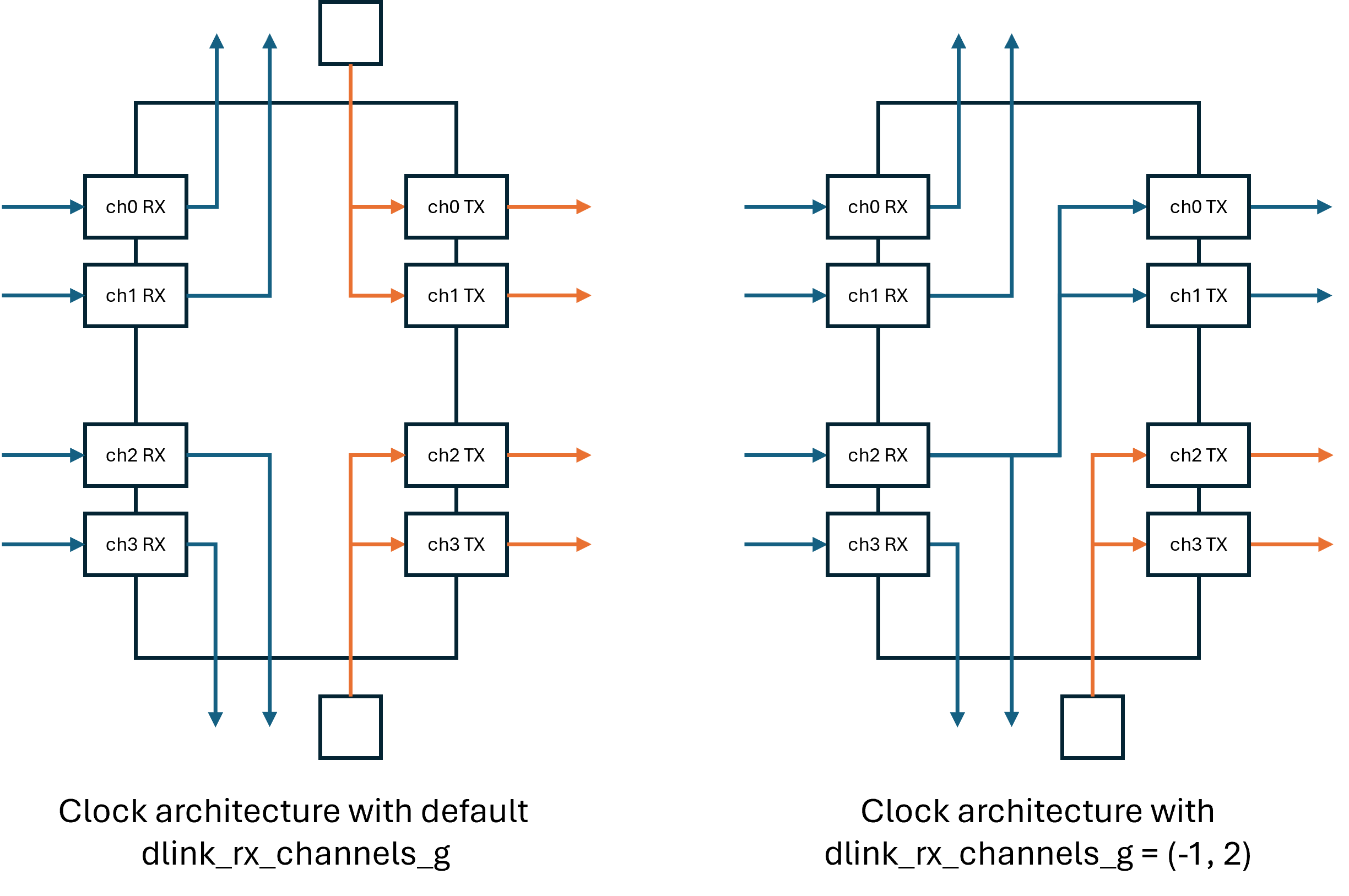
Direct Link mode can be enabled by editing the dlink_rx_channels_g generic. This alters the clock routing at the interface between FPGA fabric and transceiver resulting in an alternate configuration.
As explained in the “Clocking” section below, by default transmissions on each dual are driven by the respective dcuN_clk_i provided by the user. If a Direct Link to a dual is enabled by setting the corresponding element of dlink_rx_channels_g to an integer between 0 and 3 (both included), the chN_rx_clk_o corresponding to the selected number will be used for transmission in both channels of the selected dual.
The intended purpose of this feature is the establishment of a chain of modules that exchange information synchronously with the same oscillator, ensuring (as an example) that no samples are lost in remote ADCs. Currently the correct functionality of such a chain is only verified in the case of a point-to-point connection between a HotRIO master board and a HotRIO slave board.
Note that the Direct Link is only needed on the HotRIO slave board, as the master does not need to reply synchronously with received data. Moreover, if CTC (Clock Tolerance Compensation) is enabled in the HotRIO slave module, there is no need for a Direct Link, as CTC will transfer received data to the local clock domain before providing it to the HotRIO slave output (this may result in loss or duplication of samples in remote ADC applications, but the frequency of these effects is related to the PPM tolerance of the local oscillators, and it is negligible for most applications).
When Direct Link is enabled for a dual, the tx_data_i and tx_kchar_i of its two channels must be synchronous to the chN_rx_clk_o specified in the dlink_rx_channels_g generic. Typically this is accomplished by connecting the HotRIO slave module’s clk_i port to the RX clock provided by the Quad Wrapper. This may require other logic for payload and sideband data generation to be synchronous with the RX clock. When designing a Direct Link application, be mindful of the intermittent nature of this clock, as it may be interrupted if the corresponding RX fiber is damaged or disconnected.
The following diagram exemplifies the meaning of the DIrect Link option by comparing the resulting clock distribution network with its default value (-1, -1) and with the value (-1, 2):
Enabling and disabling channels
The rx_enable_g and tx_enable_g generics can be used to disable unused channels permanently at compilation time. Each channel marked with a “0” in these generics will not be usable in the inferred Quad Wrapper, as its data paths and reset logic will not be generated to save FPGA resources. All ports referring to a disabled channel in the portlist (for example those that start with “ch1_tx_” if tx_enable_g="1101") shall be kept at default or unspecified if they are inputs, and they shall be ignored or unspecified if they are outputs.
If both channels of a dual are disabled both in tx_enable_g and in rx_enable_g, the dual will not be instantiated in the Quad Wrapper and the width of the “hdin” and “hdout” ports will be reduced to 2. It is invalid to disable all channels both in RX and TX, as this would result in the elimination of the entire logic of the Quad Wrapper.
Enabled channels can still be powered up or down at runtime depending on firmware necessities. To do so, the user may control the chN_rx_pwrup_i and chN_tx_pwrup_i inputs. Note that these inputs are set to “0” by default; as a result, if they are left unspecified the corresponding channels will be powered down even if they were enabled in the generics. If a channel should always be active, its “pwrup” signal should be tied high in the port map.
Inverting channels
The Quad Wrapper provides the rx_invert_g and tx_invert_g generics to invert the serial data inputs or outputs of the transceiver, changing zeros to ones and vice versa in the 10-bit characters of 8b/10b.
This feature can be used to compensate for reversed differential pair connections between the FPGA and the fiber optic transceiver on the target hardware.
Setting the size of reset counters
Finally, the generic list provides a series of configurations to change the behaviour of the internal reset state machine of the Quad Wrapper. For most synthesizable applications, it is suggested to omit these settings in the generic map. Default values are tested and will guarantee the acquisition of a stable lock of the TX PLL and of the CDR (Clock and Data Recovery) PLLs as long as stable reference clock and data streams are provided to the module.
For simulation purposes, it may be beneficial to tweak some parameters to prevent the long times needed to ensure lock quality from stalling the execution of more meaningful parts of the simulation. The “detailed portlist” section above explains the meaning of each reset counter generic, but this section proposes three common tweaks to apply to accelerate lock acquisition at the expense of lock quality, under the assumption that the testbench does not need to simulate the loss of lock scenario:
generic map (
  ...
  dcu_lol_size_g     => 6,
  tx_pcs_lock_bits_g => 8,
  rx_pcs_lock_bits_g => 8
)
Summary: Quad Wrapper instantiation procedure
The following procedure exemplifies the process of instantiation of a Quad Wrapper module:
Set DCU frequencies if any are different from 125 MHz, then set Direct Links if needed.
Set rx_enable_g and tx_enable_g to the desired values depending on what channels will be used in the design.
Set rx_invert_g and tx_invert_g according to the hardware targeted by the design.
Optionally, lower
dcu_lol_size_g,tx_pcs_lock_bitsand/orrx_pcs_lock_bitsfor simulation only, to reduce simulation time.Add the hdin and hdout signals to the port map and connect them with top level ports.
For each dual that has at least one TX and/or RX channel enabled, add the corresponding “DUAL N” section of the portlist to the port map. Note that
dcuN_tx_sync_iis not needed in most applications and may be omitted if it does not need to be used.For each enabled channel, add the corresponding “CHANNEL N” section of the portlist to the port map. If running disparity controls or BIST are not needed, these subsections of the portlist can be omitted. Ports starting with “chN_rx” or “diag_chN_rx” shall only be added if the RX is enabled for the channel; those starting with “chN_tx” only if the TX is enabled. For most applications the
chN_tx_idle_ican also be omitted.
Clocking guidelines
While the Quad Wrapper is designed to require only one clock input per Dual (dcuN_clk_i), the internal DCUA primitive components require and generate several clocks whose connections are handled by the Quad Wrapper based on assumptions on the most common use cases of the module in the HotRIO environment.
The following 10 clocks are defined inside the Quad Wrapper module:
RX reference (one per Dual): these clocks serve the purpose of keeping the CDRs close to the target frequency for a faster lock acquisition once data is available on hdin, and they are used in SerDes/PCS reset logic.
TX reference (one per Dual): these clocks drive the TX PLLs of the Duals, which generate the fast “bit clocks” for serial data on hdout and the slower TX pclks for parallel data in the TX paths.
TX pclk (one per Dual): these clocks drive parallel data in the PCS and SerDes TX datapaths. They are also used in the pcs_lol_detector core to identify the lock status of the TX PLLs.
RX pclk (one per channel): these clocks are generated by the CDRs and they are synchronous with incoming RX data on each channel. In the Quad Wrapper they are provided to the user on
chN_rx_clk_oand they drive the diagnostic counters of the channels.
Reference clocks
RX references and TX references are directly connected to other primary clocks and they do not need to be defined by the user in the timing constraint files. RX reference is always directly connected to dcuN_clk_i, while TX reference is connected to dcuN_clk_i in normal operation conditions, but it is instead driven by the RX pclk of channel N if a Direct Link with channel N is enabled.
Note
The dcuN_clk_i is connected to the RX reference of the Dual, whose stability must be guaranteed after the transient phase following FPGA boot to allow correct lock detection and reset of the subsystems of the transceiver. Accordingly, each dcuN_clk_i must be assigned by the user to a stable local clock matching the frequency of the Dual.
Regardless of the operation mode, TX data and K-character flags must always be provided to the Quad Wrapper synchronously with the TX reference. As a result, in normal operation mode they shall be synchronous to dcuN_clk_i, while in Direct Link mode they shall be synchronous to chN_rx_clk_o.
TX pclks
TX pclks are only used internally in the Quad Wrapper and they are related to the TX references, but Lattice Diamond cannot infer their frequencies. Accordingly, each TX pclk needs to be defined by the user in the timing constraint files, unless TX is disabled through tx_enable_g for both channels of its Dual. To define the clocks, apply the period or frequency constraints to the following signals:
quad_wrapper_inst/tx_pclk_s[0]
quad_wrapper_inst/tx_pclk_s[1]
replacing quad_wrapper_inst with the instance name of the Quad Wrapper module in the design. If the Quad Wrapper is defined as a submodule of another module instead of being directly instantiated in the top level, use a hierarchical name for the instance.
RX pclks
RX pclks are used both inside and outside the Quad Wrapper. Being synchronous with RX data of their channel, they must be retrieved from the chN_rx_clk_o ports and used in any modules that directly manipulate RX data. If RX data needs to be forwarded to a TX path, with or without modifications, it shall be crossed from the RX pclk domain to the TX reference domain. In the HotRIO environment there are two proposed approaches to do so:
In normal operation mode, a HotRIO CTC FIFO can perform the clock domain crossing on a HotRIO data stream even if the two domains are unrelated, preserving the average arrival frequency of HotRIO packets of the data source. To instantiate it, connect the RX data to a HotRIO Slave with
ctc_gset to true.Alternatively, a Direct Link can be enabled between the RX channel and the TX Dual. In this case the RX pclk and the TX reference are assigned to the same signal and no clock domain crossing is needed.
As all RX pclks corresponding to enabled RX channels need to be used in the firmware, they need to be defined in the timing constraint files. To do so, apply the period or frequency constraints to the following signals:
quad_wrapper_inst/ch0_rx_clk_o
quad_wrapper_inst/ch1_rx_clk_o
…
Note
Sometimes Lattice Synthesis Engine may assign different names to the primary clock nets representing the RX pclks. Always check the Place & Route report to make sure that constraints have been properly understood.
Warning
RX pclks are bound to CDR status. They may be interrupted when a fiber is disconnected or an upstream node stops transmitting, and they may not respect their own frequency constraint when the CDR is unlocked. Whenever chN_rx_ready_o goes from low to high, any logic connected to a chN_rx_clk_o must be reset to a known stable state before being used.
Reset and Readiness
For each Dual, the wrapper contains reset sequencing for the shared TX path and each RX channel. Power-up inputs are asynchronous and active high, while reset inputs are synchronous to dcuN_clk_i and active low. The ready outputs indicate whether the associated datapath is expected to be usable:
dcuN_tx_ready_oindicates that the TX reset sequence for Dual N has completed and that transmitted data is expected to be received unchanged in the downstream node.chN_rx_ready_oindicates that the RX reset sequence for channel N has completed and that received data is expected to be valid.When a ready output is low, the corresponding clock may be absent or unstable and datapath contents should be treated as invalid.
Datapath
Each channel exposes:
8-bit TX data input and 8-bit RX data output.
TX and RX K-character flags.
TX idle and disparity-control inputs.
Optional RX polarity inversion and TX polarity inversion through generics.
Built-In Self Test (BIST) generator on the TX path and checker on the RX path.
Diagnostic counter for RX 8b/10b protocol errors.
Built-In Self Test (BIST)
Each channel includes the BIST enable runtime setting and the BIST active and error flags.
The BIST enable inputs are synchronized internally before driving the BIST pattern generator/checker logic. By default, they are kept low, disabling BIST functionality altogether. This can be overridden by the user by connecting BIST enable to a high value or to a control signal.
When BIST is enabled for channel N, data on chN_tx_data_i and chN_tx_kchar_i is ignored by the Quad Wrapper. If a design only uses BIST and does not need to transmit any other kind of data, the datapath ports may be omitted from the Quad Wrapper portlist.
Even if enabled, BIST modules cannot run until the relevant ready flag is high (TX ready for BIST generator, RX ready for BIST checker). When the BIST checker begins running, it looks for the character sequence D0.1 D0.2 D0.3. When it finds it, it goes to the active state and chN_bist_active_o goes high. From there onwards, every time the received character does not match the expected character in the BIST sequence, chN_bist_err_o goes high for one clock cycle.
Both output flags of the BIST checker module are synchronous to chN_rx_clk_o.
Diagnostics
The diagnostic outputs report accumulated RX errors per channel using counters of width defined by the global CONFIG_DATA_WIDTH setting. The errors are counted and provided to the user in the chN_rx_clk_o domain.
Counted RX errors may be of two different types: code violation errors and running disparity errors. If a received character represents both a code violation and a running disparity error, it is counted only once.
The diagnostic counters are only updated when the respective channels are in ready state. If a channel loses readiness, its diagnostic counter is reset to zero, but the error state can be detected by inspecting the chN_rx_ready_o signal.
Description of the submodules
Note
The previous section concluded the usage guide for the Quad Wrapper module. This section provides detailed portlists and implementation details for the submodules included in the Quad Wrapper, and it is only provided for those who would like to understand the inner workings of the module or to modify it for their own purposes.
BIST gen
This module, when active, generates a ramp sequence of 8 bits from 0 to 255 and then back to 0. Comma character (K28.5) are interspersed between the ramps to allow the PCS receiving the sequence to lock onto the signal. The number of ramps between comma characters can be modified using the K_COUNTER_BITS generic. This generic changes the number of bits of the ramps counter. The comma character is sent every 2 ^ K_COUNTER_BITS ramps.
Generics
Name |
Description |
Type |
Default |
|---|---|---|---|
k_counter_bits | log2 of the number of ramps between two k28.5 insertions |
|
|
Input signals
IN ports
Name |
Description |
Type |
|---|---|---|
clk | txi clock of the pcs channel |
|
rstn | active-low asynchronous reset |
|
en | enable signal, synchronous with `clk` |
|
Output signals
OUT ports
Name |
Description |
Type |
|---|---|---|
tx_k | special character flag for the current byte in the sequence |
|
tx_data | value of the current byte in the bist sequence |
|
Implementation details
The implementation is based on two processes. The first process, when enabled and not in reset, increments a counter that has the width of the generic K_COUNTER_BITS. When the counter wraps around and assumes the 0 value, a flag is set to indicate that the next data to be transmitted is a comma character. The second process, when enabled and not in reset, uses an 8-bit counter to generate a ramp. The ramp is sent to the output when the k-character flag is not set, otherwise the comma character is sent.
BIST check
This module is intended to be used in combination with the BIST gen module. It verifies that the data received matches the pattern generated (ie a ramp sequence with comma characters). The active output notifies that the module has identified the start of the signal. While the module is active, the err signal will pulse high when a mismatch is detected between the received data and the expected data.
Input signals
IN ports
Name |
Description |
Type |
|---|---|---|
clk | rxi clock of the pcs channel |
|
rstn | active-low asynchronous reset |
|
en | asynchronous enable signal |
|
rx_k | received special character flag |
|
rx_data | received data byte |
|
Output signals
OUT ports
Name |
Description |
Type |
|---|---|---|
err | bist error flag |
|
active | bist active flag |
|
Implementation details
This module uses a very simple state machine to identify the start of the ramp. If the characters 0x00, 0x01 and 0x02 are received in sequence, the module sets the active flag high. The module then compares every received character with the expected one. If the value does not match a counter incrementing by one every cycle, the err signal is set high. Note that if the alignment between the internal counter and the data stream is lost, it can only be reobtained by resetting the whole RX channel, or by reconnecting the corresponding fiber.
LOL detector
This module compares two clocks and determines if the two clocks are locked. This is used to check if the TX PLL clock output is locked to the TX reference clock.
Generics
Name |
Description |
Type |
Default |
|---|---|---|---|
pulse_counter_size | bits of the counter over which the difference between the two clocks is accumulated |
|
|
unlock_diff | minimum difference to consider the two clocks unlocked |
|
|
lock_diff | maximum difference to consider lock reestablished |
|
|
Input signals
IN ports
Name |
Description |
Type |
|---|---|---|
refclk_rx | stable local clock matching pcs frequency |
|
refclk_tx | reference clock provided to the tx pll of the dual |
|
pclk_tx | output clock generated by the tx pll of the dual |
|
rstn | active-low reset synchronous to `refclk_rx` |
|
Output signals
OUT ports
Name |
Description |
Type |
|---|---|---|
tx_lol | loss of lock output, synchronous to `refclk_rx`. high when `pclk_tx` is not locked to `refclk_tx` |
|
Implementation details
A pulse is generated at regular intervals (2^PULSE_COUNTER_SIZE cycles) on the “refclk_tx” clock domain. The pulse is then crossed to the “pclk_tx” clock domain, where a counter runs and counts how many clock cycles have passed. If the absolute value of the difference between the length of the regular interval and the count on the potentially unstable clock “pclk_tx” is too high (higher than UNLOCK_DIFF), the PLL is considered unlocked. If the same difference goes below LOCK_DIFF, the PLL is considered locked again. At startup, or after asserting “rst”, the PLL is considered unlocked. Two heartbeat signals are also produced; one on the “pclk_tx” domain and one on the “refclk_tx” domain. Their purpose is to verify the presence of the clocks. If “pclk_tx” or “refclk_tx” are absent, the PLL is clearly unlocked; if “refclk_rx” is absent, though, this module does not operate correctly. The “tx_lol” output flag is synchronous to “refclk_rx”.
Reset state machine
Custom state machine to replace the auto-generated reset state machine of the PCS IP core. This module resets a single data path of the PCS, independently from the other. In the typical application, using both the TX and RX branch of the PCS channel, two instances of this module will be used, one for the TX path and one for the RX path. When using the module as a TX reset, follow the instructions in the comments on the entity declaration.
Generics
Name |
Description |
Type |
Default |
|---|---|---|---|
serdes_rst_counter_bits | one plus the log2 of the number of refclk cycles between rstn release and serdes_rst_out release |
|
|
pcs_rst_counter_bits | one plus the log2 of the number of refclk cycles between serdes_rst_out release and pcs_rst_out release |
|
|
lock_counter_bits | one plus the log2 of the number of refclk cycles `lol_los` must stay low for continuously to reach the ready state |
|
|
lol_counter_bits | one plus the log2 of the number of refclk cycles `lol_los` must stay high for continuously to trigger a new reset sequence |
|
|
synchronize_lol_los | if true, infer a 2-ff synchronizer in the refclk domain for the `lol_los` input |
|
|
Input signals
IN ports
Name |
Description |
Type |
|---|---|---|
refclk | rx reference clock of the dual |
|
rstn | active-low synchronous reset |
|
serdes_rst_dual_in | user request to reset the serdes block of the dual (active-high) |
|
rst_dual_in | user request to reset both the serdes and pcs blocks of the dual (active-high) |
|
serdes_rst_in | user request to reset the serdes subblock of the channel (active-high) |
|
pcs_rst_in | user request to reset the pcs subblock of the channel (active-high) |
|
lol_los | if the module is a tx reset, txpll loss of lock signal. otherwise, cdr loss of lock combined with or gate with loss of signal flag |
|
Output signals
OUT ports
Name |
Description |
Type |
|---|---|---|
serdes_rst_out | serdes reset for the dcu channel |
|
pcs_rst_out | pcs reset for the dcu channel |
|
word_align_en_out | word alignment enable signal for the dcu channel |
|
ready | readiness indicator for the user. if high, data can be exchanged on the channel with no losses or distortions |
|
Implementation details
The module functionality is implemented using a state machine. A second process is used to check the stability of the pll lock.
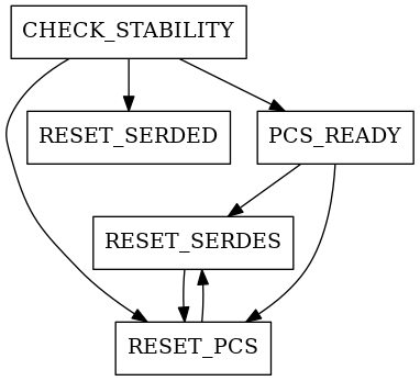
The state machine has the following states: RESET_SERDES, RESET_PCS, CHECK_STABILITY and READY. At powerup or after asserting “rst”, or any serdes rst, the machine is in the RESET_SERDES state. The RESET_SERDES and RESET_PCS states last until the completion of the corresponding counters. The state of the link is monitored through the “lol_los” variable. While the former is high, an internal lol_counter is incremented; if it finishes, the PLL is considered lost and the state goes back to SERDES_RST. While it is low, an internal lock_counter ticks instead, and if it finishes the state can change from CHECK_STABILITY to READY. If code violation or running disparity errors have been detected in large numbers, the PCS is considered unstable and the state goes back to RESET_PCS. This check is performed externally and communicated to the state machine through the “pcs_rst_in” port.
PCS error counter
Counter module used to keep track of the number of errors detected in the PCS receiver.
Generics
Name |
Description |
Type |
Default |
|---|---|---|---|
rst_cnt_bits_g | log2 of the no. of errors that, if received over the duration of a 18-bit counter, will trigger an automatic pcs reset |
| Unspecified |
Input signals
IN ports
Name |
Description |
Type |
|---|---|---|
rx_pclk_i | rx clock generated by the pcs |
|
rstn_i | active low asynchronous reset |
|
rx_err_i | code violation error or running disparity error |
|
Output signals
OUT ports
Name |
Description |
Type |
|---|---|---|
auto_reset_o | pcs reset issued if too many errors are detected in a short time |
|
rx_err_cnt_o | number of errors detected since last reset |
|
Implementation details
The module contains a counter whose width is determined by the CONFIG_DATA_WIDTH global setting. Its value is incremented whenever a code violation error or a running disparity error is detected. The module also controls an automatic PCS reset mechanism by checking the number of errors over a period of 2^18 clock cycles; the reset is asserted if this number gets past 2^(rst_cnt_bits_g) - 1.