VSPI
The ‘vSPI’ module enables multiplexing of the SPI interface between the FPGA and an external MCU to other SPI slaves. This module needs to be directly connected to the SPI output port. Externally, it includes the standard SPI pins: CLK, MISO, MOSI, and CS, as well as a special Chip Select (vCS) for the virtual SPI devices. The primary internal interface has higher priority over the virtual devices; if the main chip select is asserted, it takes precedence regardless of the virtual device’s status. If neither main nor virtual chip select are asserted, the MISO line is placed into a high impedance state, so that the MCU can use it to communicate with the FPGA at startup. The selection of a vSPI device is controlled via an external input, typically linked to a register.
To communicate with a virtual SPI slave, follow these steps: - Use the standard FPGA interface to set the appropriate index on the vSPI register. - When the primary CS is deasserted and the vSPI CS is asserted, the port is connected to the SPI device selected by the index. - At any time, the main CS can be asserted to interact with the FPGA’s registers. This can happen even while the vCS pin remains asserted, as the main CS always takes priority.
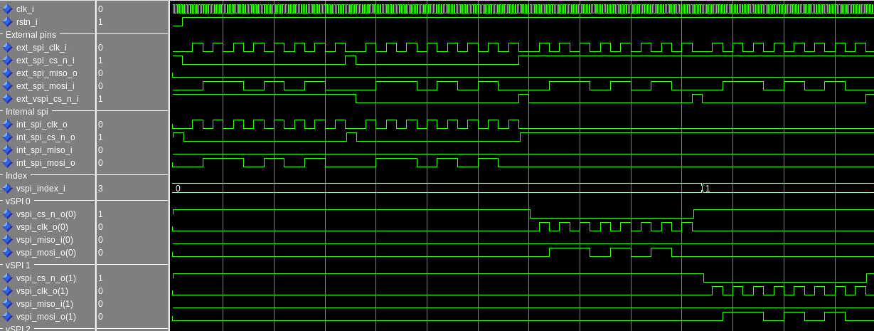
When interfacing with a slave device that supports only half-duplex communication (where MISO and MOSI share the same pin), these two functions can be mapped to separate virtual devices. Additional logic is required to switch the I/O mode of the external pin and to OR the two CS signals. However, this module ensures glitch-free switching of the virtual devices’ CS by synchronizing changes with the FPGA clock, guaranteeing smooth transitions, albeit with a potential additional latency of up to one clock period.
To communicate with such a half-duplex device, follow these steps: - For example, map the MOSI mode to index 0 and the MISO mode to index 1. - The MCU interacts with the FPGA to set the vSPI index to 0. - The primary CS is deasserted, and the vSPI CS is asserted. After a brief delay, the corresponding CS becomes active, allowing communication to begin. - The MCU sends a command to the slave, managing the clock and MOSI line. - Once the MCU finishes its transmission and awaits a response, it asserts the main CS while keeping the vCS asserted. - The MCU then commands the FPGA to change the vSPI register to index 1. - The MCU can now continue communication, providing a clock to the slave so it can send its response.
Ports
Name |
Description |
Type |
|---|---|---|
clk_i |
Input clock signal for synchronization |
std_logic |
rstn_i |
Active-low synchronous reset signal |
std_logic |
vspi_index_i |
Index input to select the active vSPI device |
std_logic_vector(CONFIG_DATA_WIDTH - 1 downto 0) |
ext_spi_clk_i |
External SPI clock input |
std_logic |
ext_spi_miso_o |
External SPI Master In Slave Out output |
std_logic |
ext_spi_mosi_i |
External SPI Master Out Slave In input |
std_logic |
ext_spi_cs_n_i |
External SPI Chip Select (active low) input |
std_logic |
ext_vspi_cs_n_i |
vSPI Chip Select (active low) input for selecting vSPI devices |
std_logic |
int_spi_clk_o |
Internal SPI clock output |
std_logic |
int_spi_miso_i |
Internal SPI Master In Slave Out input |
std_logic |
int_spi_mosi_o |
Internal SPI Master Out Slave In output |
std_logic |
int_spi_cs_n_o |
Internal SPI Chip Select (active low) output |
std_logic |
vspi_cs_n_o |
Output vector for vSPI Chip Select signals for multiple devices |
std_logic_vector(vspi_devices - 1 downto 0) |
vspi_clk_o |
Output vector for vSPI clock signals for multiple devices |
std_logic_vector(vspi_devices - 1 downto 0) |
vspi_miso_i |
Input vector for vSPI MISO lines from multiple devices |
std_logic_vector(vspi_devices - 1 downto 0) |
vspi_mosi_o |
Output vector for vSPI MOSI lines to multiple devices |
std_logic_vector(vspi_devices - 1 downto 0) |
Implementation Details
Multiplexer and Demultiplexer Logic
The multiplexer and demultiplexer components within the vspi module are purely combinational and operate independently of the FPGA clock. The combinational logic dynamically selects which SPI lines are connected based on the state of the vSPI index. This ensures that the communication speed is not dependant from the internal FPGA clock.
Synchronous CS
The vSPI CS control logic is synchronized with the FPGA clock to avoid glitches during the switching process. This is useful when a single device is mapped to multiple vSPI ports, for example when a device that supports only half-duplex SPI is mapped to two vSPI ports.