ADC36xx Interface
This module is used to decode the data from the ADCs of the 366x of 368x family from Texas Instruments.
These ADCs use an interface with 1, 2 or 4 differential pairs + one for the “frame clock” that delimits the start and the end of the data. This module supports the decoding of all three modes of operation, namely 1/2-wire, 1-wire and 2-wire modes. The ADCs can be also configured to truncate or average the sampled data, resulting in a variable length data that can be 14, 16, 18 or 20 bits long. Also all these modes are supported by the following module.
The mode of operation can be changed on-the-fly without a need for recompilation, but the ADC interface should be reset after doing so. Similarly, a reset is needed whenever a new configuration is uploaded on the ADC device’s register map.
The modes are defined by the following constants, declared in the globals:
constant bit_mode_14_c : std_logic_vector(1 downto 0) := “00”;
constant bit_mode_16_c : std_logic_vector(1 downto 0) := “01”;
constant bit_mode_18_c : std_logic_vector(1 downto 0) := “10”;
constant bit_mode_20_c : std_logic_vector(1 downto 0) := “11”;
constant wire_mode_2_c : std_logic_vector(1 downto 0) := “00”;
constant wire_mode_1_c : std_logic_vector(1 downto 0) := “01”;
constant wire_mode_1_2_c : std_logic_vector(1 downto 0) := “10”;
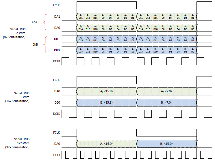
Bit modes select the number of bits in each sample retrieved from the ADC, while wire modes define how data is communicated from the ADC to the FPGA. 1-wire and 1/2-wire modes can be used to reduce the number of needed connections between ADC and FPGA at the cost of higher data clock frequency. If this is not strictly needed, it is suggested to operate the ADC interface in 2-wire mode to simplify timing closure in the design.
Additional support modules
It must be noted that this interface does not provide all the needed support to operate ADC36xx devices. Additional support interfaces may be provided inside or outside FPGA fabric, and they consist of clock generation and SPI configuration.
ADC clock generation
According to the datasheet, the user shall provide two related clocks to the ADC device:
The sampling clock (or sclk) is a single data rate clock that will trigger the acquisition of a sample from the ADC analog inputs. Its frequency can be freely chosen by the user in the limits allowed by the datasheet.
The data clock (or dclk) is a double data rate clock used by the ADC to drive data serialization and transmission processes. Its frequency shall be a specific value, selected based on the sclk frequency, wire mode and bit mode, according to the following equation:
where D is the data clock frequency, B is the bit mode value, W is the wire mode value, and S is the sampling rate, given by sampling clock frequency divided by decimation.
The table below can be used to compute the required data clock frequency in all possible bit/wire mode combinations. More information on wire modes is given in the Wire mode timing diagrams section.
|
|
ADC register map SPI configuration
For this module to be able to retrieve data from the ADC device, its operation mode must be coherent with the settings loaded onto the ADC internal register map. These can be provided and modified using an SPI interface whose details are available in the ADC datasheet.
The vspi module can be used to route SPI communication from an external source to a specific ADC device depending on a user-controlled index signal.
In configuring the register map, care must be taken to select the desired wire mode and bit mode in all registers that mention one of these settings, including those whose functions are supposed to be disabled by other registers. This guarantees maximum probability of a successful outcome, but it is still recommended to test any new configuration thoroughly.
Ports
Name |
Description |
Type |
|---|---|---|
clk_i |
Input clock signal for synchronization |
|
rstn_i |
Active-low synchronous reset signal |
|
clk_aux_i |
Auxiliary clock for the oversampling. Must be 4x the data clock. |
|
wire_mode_i |
Selects the wire mode configuration (2-bit input) |
|
bit_mode_i |
Selects the bit mode configuration (2-bit input) |
|
dclk_i |
data clock received from the ADC |
|
fclk_i |
Input vector for frame clock signals coming from the ADC |
|
da0_i |
Input data line A0, used in all wire modes |
|
da1_i |
Input data line A1, used in 2-wire mode |
|
db0_i |
Input data line B0, used in 2-wire and 1-wire modes |
|
db1_i |
Input data line B1, used in 2-wire mode |
|
data_a_o |
Output data vector for channel A |
|
data_b_o |
Output data vector for channel B |
|
valid_o |
Output signal indicating the validity of the output data |
|
sync_o |
State machine synchronization status output |
|
cnt_frame_err_o |
Output counter for frame error detection, initialized to zero |
|
Clock inputs
The module requires four input clocks to decode ADC data.
clk_ishould be the main clock domain of the FPGA design, where retrieved data will be processed. All output ports of this module are updated synchronously with this clock.fclk_igives the interface information on how samples are framed in the continuous data stream. Although it is a clock signal, it is not treated as such in the FPGA, as it does not drive the clock pin of any sequential elements. It is produced by the ADC device and its frequency is the same as the sampling rate in 1-wire and 1/2-wire modes, or double the sampling rate in 2-wire mode.dclk_iis a DDR clock whose edges signal a single bit arrival on all active data lines. The current implementation of this module does not use this as a clock, instead relying on its values to enable acquisitions in theclk_aux_idomain. It is produced by the ADC and it is locked to the data clock given to the ADC from the FPGA.clk_aux_iis used to trigger acquisition of single bits from the LVDS pairs connected to the ADC. It must be related todclk_i, multiplied by a factor of 4. This is typically accomplished by generating it in the same PLL that provides the sampling clock and the data clock to the ADC.
Data inputs
The four input data lines are meant to be connected to differential pairs receiving data from the ADC devices. These inputs are interpreted in a different way depending on the wire mode, as reported in the following table.
2-wire |
1-wire |
1/2-wire |
|
|---|---|---|---|
da0_i |
Channel A, 1st wire |
Channel A |
Channels A/B, alternating |
da1_i |
Channel A, 2nd wire |
Leave unconnected |
Leave unconnected |
db0_i |
Channel B, 1st wire |
Channel B |
Leave unconnected |
db1_i |
Channel B, 2nd wire |
Leave unconnected |
Leave unconnected |
Data outputs
When valid_o is high, data is available on both channels (data_a_o and data_b_o).
As long as the state machine is synchronized, valid data is expected once per frame clock period in 1-wire and 1/2-wire, and twice per frame clock period in 2-wire.
Since the bit mode can be changed in real time, without recompilation, the width of the output bus on each channel is fixed to the maximum possible value of 20 bits. When the bit mode is not 20-bit, the LSBs are zero-padded. For example, the 16-bit measurement 0x2A34 will be available at the channel output as 0x2A340.
Implementation Details
The module’s implementation is divided into two main parts: data acquisition and data decoding.
Data Acquisition
The data acquisition process, performed by the adc_interface_os module, is organized into three main stages:
Signal Synchronization: In the first stage, signals are synchronized within the FPGA domain to avoid metastability conditions. This is achieved using a CDC (Clock Domain Crossing) module, which also detects rising and falling edges in the data clock received from the ADC.
Phase Shift: The second stage involves a module that introduces a one-clock cycle delay to the rising and falling edge signals, creating a 90-degree phase shift.
Data Sampling: In the final stage, data is sampled on both the rising and falling edges of the clock. During the rising edge, the last two received bits are written to the output, and the valid_o flag is asserted for one clock cycle.
All outputs of the data acquisition module, namely the frame clock, the valid signal and a 2-bit data buffer for each used
differential pair, can be connected to a dual-clock FIFO to reduce the signal frequency, using the valid_o signal as a write enable.
This is the default option; as an alternative, the FIFO can be bypassed setting the enable_fifo_bypass generic to true.
It is not recommended to do so. By using the FIFO, the state machine clock clk_i only needs to be fast enough to read data at each
valid_o pulse, and it is not otherwise constrained.
Data Decoding
The data decoding process relies on a state machine with four states: SYNC, FRAME_HIGH, FRAME_MID, and FRAME_LOW. The state machine is activated only when the valid_i input is asserted, indicating the availability of new data. During this time, incoming bits are stored in a shift register, and the state machine uses the frame clock and configuration settings to output the data at the correct times.
SYNC State: After a reset or desynchronization, the state machine enters the SYNC state. It waits for the frame clock buffer to reach a “11” status, indicating that the frame clock was high during both the last rising and falling edges of the data clock. The frame clock cannot transition from low to high during the falling edge of the data clock. Upon detecting this condition, the state machine transitions to the FRAME_HIGH state. The sync_o flag, representing synchronization status, is cleared upon entering this state and it is set when data is made available in an output channel.
FRAME_HIGH State: In this state, the state machine counts a specific number of clock cycles during which the data is sampled. This number depends on bit mode and wire mode settings. It continuously checks that the frame clock remainsin the “11” status. If not, the state machine returns to the SYNC state. The behavior in FRAME_HIGH varies depending on the configuration. At the end of the counter, for incoming data sizes of 16 or 20 bits, or for any size in 1/2-wire mode, the next state is set to FRAME_LOW. In 2-wire mode the sampled data is output and the valid_o flag is asserted for one clock cycle. For data sizes of 14 or 18 bits in 1-wire or 2-wire modes, an additional state (FRAME_MID) is required between FRAME_HIGH and FRAME_LOW because the frame clock transitions to a “10” status, indicating that data from one sample is received alongside the start of the next sample’s data.
FRAME_MID State: This state is only entered in 2-wire or 1-wire mode with 14-bit or 18-bit samples. It only lasts for one data reception operation, in which both the final part of one sample and the initial part of the following one are acquired. At the following count, the state will be FRAME_LOW unless the frame clock buffer reports an incorrect value instead of the expected “10”. In 2-wire, the first sample becomes valid for both channels in this state, and as such it is output, taking care to exclude the bits that belong to the next sample.
FRAME_LOW State: This state operates similarly to the FRAME_HIGH state, except that the frame clock is checked against the “00” value, and outputs are provided at the end of the count regardless of bit mode and wire mode. After this happens, the next state is set to FRAME_HIGH and the cycle is repeated as long as the state machine stays synchronized.
A counter is maintained and incremented each time there is an error in the frame clock, causing the state machine to reset. The state machine diagram for the ADC interface is given below.

Wire mode timing diagrams
For a better understanding of state machine settings depending on wire mode, this section presents a timing diagram for each mode. These images are extracted from the ADC366x ADC datasheet from Texas Instruments. They refer to a bit mode of 16 and they are valid either with no decimation or with real decimation.