Configuration SPI slave interface
This documentation provides an overview and description of the VHDL module that creates an SPI slave interface. The module grants access to an internal register tree through the SPI interface.
Note
The module is configured to accept addresses and data in the “Little-Endian” format. They are however converted to Big-Endian internally.
Ports
Name |
Description |
Type |
|---|---|---|
clk_fpga_i |
Input clock signal |
std_logic |
rst_i |
Synchronous reset |
std_logic |
spi_cs_n_i |
Chip select signal |
std_logic |
spi_clk_i |
SPI clock signal |
std_logic |
spi_mosi_i |
Master Out Slave In |
std_logic |
spi_miso_o |
Master In Slave Out |
std_logic |
regs_addr_o |
Output register address |
config_register_in_t* |
regs_tree_i |
Input registers interface |
config_register_out_t* |
regs_tree_o |
Output registers interface |
std_logic_vector(15 downto 0) |
*The registers interfaces are defined in the global package Here
SPI protocol
The communication protocol is straightforward and consists of three fundamental commands:
Command |
Value |
|---|---|
Set address |
“01000000” |
Read |
“00100000” |
Write |
“10000000” |
The commands are defined and can be modified in the cfg_spi_constants.vhd file.
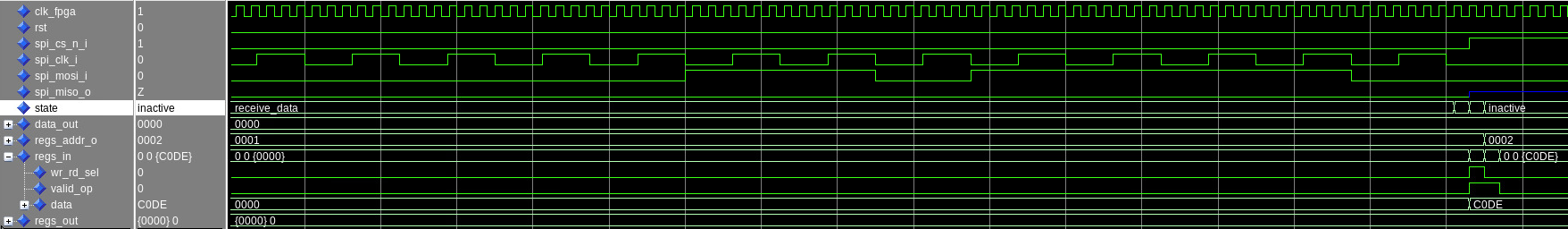
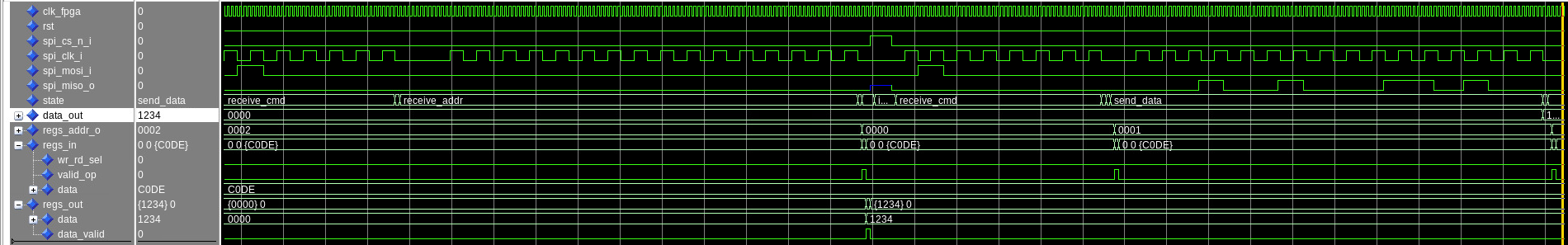
The process begins with the microcontroller sending a command, which is 8 bits long. This is followed by data transmitted in 16-bit packets, using little-endian format. Sequential reads and writes are also supported. After completing an operation, the internal address automatically increments, allowing subsequent registers to be read or written without restarting the communication process.
Note
The read operation must be always preceded by a ‘set address’ operation. If this is not performed, the data received can be outdated. This is because, to relax the timing constrains of the interface, the read operation is done when the address is changed and not when the read command is issued.

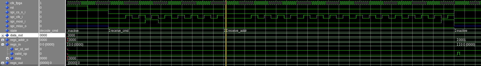
Set address operation simulation

Set address operation simulation

Set address operation simulation
Implementation details
This section provides additional details of the internal structure of the module.
Submodules
The cfg_spi module is subdivided into multiple submodules:
cfg_spi_constants.vhd contains the definition of the SPI commands and the record used to interconnect the different modules.
cfg_spi_data.vhd manages the address and the data coming from the SPI interface or the registers tree.
cfg_spi_interface.vhd implements the SPI protocol.
cfg_spi_regs_manager.vhd creates an interface for the register tree signals.
cfg_spi.vhd is the top-level module that instantiates the other modules and implements the main state machine.
SPI interface
The SPI interface operates as a module synchronized with the FPGA clock. To prevent metastable conditions, the input SPI signals undergo double-buffering. Operating at a clock frequency of 100MHz, the communication speed is capped at 16MHz. This limitation arises from the dependency on the FPGA clock.
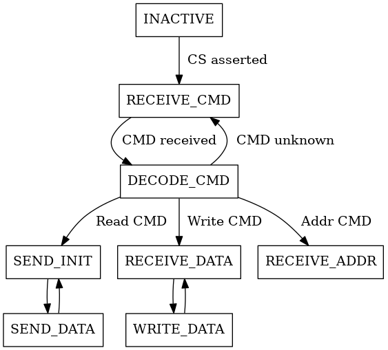
State machine
The state machine is made up of eight states:
INACTIVE, in this state all the outputs of the module are kept at zero.
RECEIVE_CMD, in this state the RX part of the SPI interface is enabled and then waits for the reception of the command. when the command has been received, it is stored inside the ‘data’ module.
DECODE_CMD, in this state, the state machine reads the received command and decides which operation to perform.
RECEIVE_ADDR, in this state the RX part of the SPI interface is enabled and then waits for the reception of the address. when the address has been received, it is stored inside the ‘data’ module.
SEND_INIT, in this state, the data that needs to be sent to the microcontroller is loaded in the TX buffer of the SPI interface. In this state, a command is also issued to the ‘data’ module to increment the address. This triggers the read of the next register from the tree. This feature enables sequential reads by preloading the data.
SEND_DATA, During this state, the data is shifted out on the MISO port following the clock provided by the microcontroller. The next state selected is SEND_INIT, which will load the next data to be sent. This is used to prepare the module in case the microcontroller wants to continue reading data.
RECEIVE_DATA, in this state the RX part of the SPI interface is enabled and then waits for the reception of the data. when the data has been received, it is stored inside the ‘data’ module.
WRITE_DATA, in this state the data received from the microcontroller is written to the register tree. The next state selected is RECEIVE_DATA, to prepare the module in case the microcontroller wants to continue writing data.
The reset and the chip select signal are used to move the state machine to the INACTIVE state. This is not displayed in the state machine diagram.